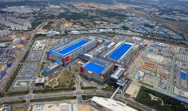
[Courtesy of Samsung Electronics]
SEOUL -- In a strategy to strengthen its foundry business in competition with Taiwan Semiconductor Manufacturing Company (TSMC), Samsung Electronics has confidently disclosed a goal to mass produce advanced semiconductors with 1.4-nanometer (nm) process technology in 2027. There has been no commitment yet from TSMC to 1.4nm chips.
A semiconductor fab or known as a foundry operates for the purpose of fabricating the designs of other companies, such as fabless semiconductor companies. Samsung has earmarked a massive preemptive investment to cement its position as the world's largest memory chip producer and enhance its competitive power in the global foundry market.
At a forum in Silicon Valley in California, Samsung revealed a roadmap to introduce its 2nm process node in 2025 and 1.4nm process node in 2027, based on gate-all-around (GAA)-based technology. GAA transistors are a modified transistor structure where the gate contacts the channel from all sides and enables continued scaling. Samsung started mass-producing the world's first 3nm process in June.
"The technology development goal down to 1.4nm and foundry platforms specialized for each application, together with stable supply through consistent investment are all part of Samsung's strategies to secure customers' trust and support their success," Samsung's foundry business head Choi Si-young said in a statement on October 4.
Samsung vowed to expand its production capacity for advanced nodes and actively target high-performance and low-power semiconductor markets while enhancing its GAA-based 3nm process support for high-performance computing and mobile.
reporter

Lim Chang-won
cwlim34@ajunews.com